
FOB Price
Get Latest Price1 USD / Piece
|100 Piece Minimum Order
Country:
China
Model No:
INMC028
FOB Price:
1 USD / Piece Get Latest Price
Place of Origin:
-
Price for Minimum Order:
1 per Piece
Minimum Order Quantity:
100 Piece
Packaging Detail:
Export Carton / Wooden Box / Pallet
Delivery Time:
30 days after payment
Supplying Ability:
20000 Piece per Month
Payment Type:
L/C, T/T, Western Union
Product Group :
Contact Person Wilson
Xiamen, Fujian
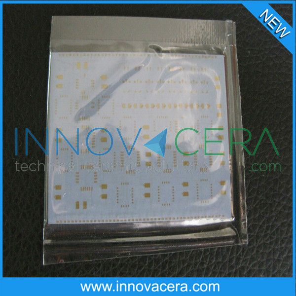
Alumina Metallized LED Ceramic Substrate
1.Good corrosion
2.Good heat conductivity
3.ISO certified Manufacturer
4.*6 Alumina
Alumina Metallized LED Ceramic Substrate
*6 alumina ceramic substrate
Ceramic substrate pcb
Innovacera provides electronic ceramic substrate including Al2O3
(Alumina substrate) and AlN (Aluminum Nitride substrate). These
ceramic substrate have good mechanical strength and abrasion
resistance, high thermal conductivity , very stable in high
temperature and corrosive chemical and excellent electrical
insulation.
Substrate made from Alumina Ceramic
Alumina ceramic is kind of structural ceramics, with insulation
resistance, voltage resistance, high strength, good thermal
conductivity, dielectric loss, stable electrical performance
characteristics. Used in electronic ceramic substrates, ceramic
electrical insulation, vacuum devices, devices porcelain, spark
plugs and other products. We can make the part by hot injection
pressing, dry pressing, isostatic pressing and extrusion productive
technology etc.
Overview of Main Physical Properties:
1.Good electrical insulation
2.High mechanical strength
3.Excellent wear resistance
4.Excellent corrosion resistance
5.Low dielectric constant
Overview of Main Applications:
1. High Power LED ceramic substrate
2. Microwave (Wireless Communication & Radar)
3. Semiconductor Process Equipment
4. Solar Cell
5. Hybrid Electric Vehicles
6. Flip chip/eutectic substrate
7. Sensor ceramic substrate
Different Kinds of Substrates:
As requested, we provide various kind of metallizations as
below:
1.Thin Film Ceramic Substrate
This product is widely used in circuit substrates for optical
storage, optical communication, RF application, LED and various
other uses.
2.Thick Film Ceramic Substrate
This product is widely used in circuit substrates for optical
storage, optical communication, RF application, LED and various
other uses.
3.High Temperature Co-fired Substrates (HTCC)
This product achieves a variety of products with high reliability,
high density, and multifunction. It is used in ceramic heater,
optical/power element package, and sensor package.
Difference between thin & thick film patterns
Thin Film Patterns
Thick Film Patterns
Better pattern accuracyof +/*1%
Normal Pattern accuracyof +/**0%
Higher surface roughness of <0.3um
Poor surface roughness of 1~3um
Goodsurface adhesion in both Al2O3 and AlN
Good surface adhesion in Al2O3 but poor adhesion in AlN
Good alignment accuracy
Poor alignment accuracy
Higher materialstability (Cu layer)
Normal materialstability (Ag and glass mixture)
Conductivity Comparison of Various Materials
Materials
Conductivity(W/mK)
FR4
0.2
Al2O3
****7
Aluminium Nitride(AlN)
******0
Gold
**5
Silver
**5
Copper
**8
Material Specifications&Properties
We can supply the products according to customer's drawings,
samples and performance requirements.
Material
Unit
Al2O****7
Al2O****3
Al2O****0
Items
Al2O3
%
*9.7
*9.3
*5
Density
g/cm3
3.*5
3.*8
3.2
Water Absorption
%
0
0.*1
0.2
Flexural Strength
Mpa
**0
**0
**0
*0°C Leakage rate
Torr/L.sec
<****1
<****1
<****1
High Temperature Curve
mm
***0°C
0.2mm is allowed
***0°C
0.2mm is allowed
***0°C
0.2mm is allowed
High Temperature Bonding
***0°C
Not
***0°C
Not
***0°C
Not
*0~***0°C Coefficient of Linear Thermal Expansion
mm.***6/°C.m
8.6
8.2
8.2
Thermal Conductivity
W/m.K
*5
*5
*0
Breakdown Voltage
KV/mm
*0
*0
*5
*0°C DC Volume Resistivity
Ohm/cm
***4
***4
***4
High Temperature Volume Resistivity
***0°C M?
?0.*8
?0.*8
?0.*8
***0°C M?
?0.*2
?0.*2
?0.*2
***0°C Thermal Shock
?
Did not crack
in 6 times cycle at ***0°C
Did not crack
in 6 times cycle
at ***0°C
Did not crack
in 3 times cycle
at ***0°C
Limit of Application
°C
***0
***0
***0
Max Manufacturing Length for Tube
mm
***0
***0
***0
Overall Production Process:
Factory Tour:
Quality Control/Assurance Standard:
We are ISO certified: ISO***1:***8 ISO****1:***4
OHSAS****1:***9
The constant goal of Innovacera is a superior level of quality and
sevice at competitive prices. Particular attention is given to the
production of individual customer parts for both large and small
runs. We implement a very sophisticated Quality Control process
which we have our own customers certify. All parts that pass
through our facility are visually and dimensionally inspected as
well as calibrated. Our engineering staff is available for counsel
and recommendations that will satisfy your ceramic
requirements.
Superior quality of products with reliance is our prime
consideration.
Feel free to contact us if you need any other assistance about our
products.
We care and provide what you want!
| Country: | China |
| Model No: | INMC028 |
| FOB Price: | 1 / Piece Get Latest Price |
| Place of Origin: | - |
| Price for Minimum Order: | 1 per Piece |
| Minimum Order Quantity: | 100 Piece |
| Packaging Detail: | Export Carton / Wooden Box / Pallet |
| Delivery Time: | 30 days after payment |
| Supplying Ability: | 20000 Piece per Month |
| Payment Type: | L/C, T/T, Western Union |
| Product Group : | Metallized Ceramics |