
FOB Price
Get Latest Price|
- Minimum Order
Country:
India
Model No:
-
FOB Price:
Place of Origin:
-
Price for Minimum Order:
-
Minimum Order Quantity:
-
Packaging Detail:
-
Delivery Time:
-
Supplying Ability:
-
Payment Type:
-
Product Group :
Contact Person Vikash
Opposite Citi Mall, New Link Road, Andheri - West, Mumbai, Maharashtra
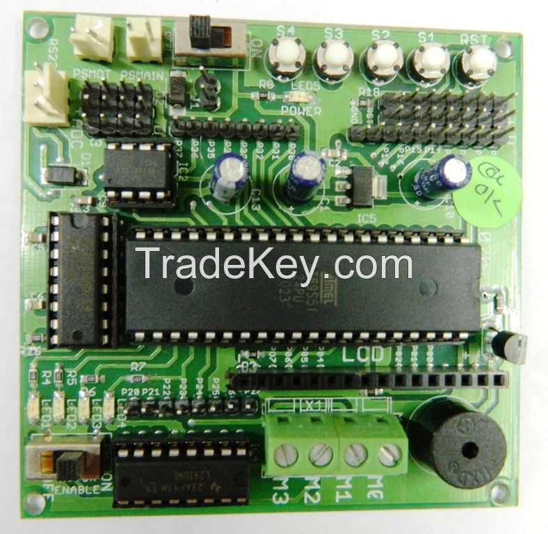
1. ***1 Development board (*****1):
1.1. Features
***1 development board is a ***1 micro controller based mother
board. It can be use for various embedded system development
applications and in the field of robotics as a brain of the robot.
This board have the following features.
Compatible with most of the ***1 and ***2 series of *0 pin
microcontrollers.
Available with NXP P*9v*1rd2 micro controller
On board motor driver for driving 2 DC motors or 1 stepper
motors
Motor enable disable control switch
Onboard 4 channel ADC optional
LCD interface
PC interface through UART
*1.***2 MHz crystal
Exposed all I/O port for general-purpose
application
five tact switches for external , reset and
interrupt
Four test LEDs for status and debugging purpose
Buzzer for generating audible response
Exposed ISP pins for Programming
on board programmer for p*9v*1rd2 microcontroller
On board regulated power supply
Dual power supply for logic and driving load
1.2 Parts description and connection
details
Voltage Regulator
Here IC***7 is used as a voltage regulator. It is a 5V voltage
regulator IC used to provide a constant voltage of 5Vto the micro
controller and other peripherals attached in the main
board.
Level converter
Here IC **2 is used it is basically use to connect the motherboard
with the PC. It provides a voltage level conversion in between the
serial port of PC and serial port of our
motherboard.
Motor Driver
Here IC L**3NE is used as a motor driver. It takes from micro
controller and can able to drive high current high voltage
inductive loads, relays, solenoids, DC motors and stepper motors.
The L**3NE is a high-current H bridge driver. The L**3NE is
designed to provide bidirectional drive currents of up to ***-mA at
voltages from 4.5 V to *6 V. The connection details of this IC is
given below
In*- Port2_4 Out *- M0
In*- Port2_5 Out *- M1
In*- Port2_6 Out *- M2
In*- Port2_7 Out *- M3
Buzzer
Active low It can be easily use to get audible response from the
controller. The connection details is given below.
Port0_3
Serial port
This is use to download program in the micro controller through PC
and can be use to communicate with the PC through
UART.
LCD interface
It can be used to interface a*6x2 LCD in 4 bit mode or it can also
be used as a general purpose output port. The pin connections
for interfacing a LCD are given bellow.
RS- Port0_0
RW- Port 0_1
E- Port0_2
D*- Port0_4
D*- Port0_5
D*- Port0_6
D*- Port0_7
Switches
S*-Port3_2
S*-Port3_3
S*-Port3_4
S*-Port3_5
These switches are connected to port pins of micro controller to
give external s and interrupt. All this switches are active
low. RST-Reset This switch can be use to reset the micro
controller. POWER-Power on This is basically a slide switch. It is
use to switch on or off the main power supply of the motherboard.
MOTOR ENABLE This is basically a slide switch. It is use to enable
or disable the motor driver.
LEDs
LED*-Port2_0
LED*- Port2_1
LED*-Port2_2
LED*-Port2_3
These LEDs are connected to port pin in active high mode.
LED*-Power ON/OFF indicator LED
PSMAIN
This is use to connect power supply to the Main board (minimum 6VDC
maximum *6VDC)
PSMOT
This is use to connect power supply to the motor (minimum 5VDC
maximum *2VDC)
2. The P*9v*1RD2 Microcontroller
2.1 Description
The P*9V*1RD2 is an *0C*1 microcontroller with *4 kB Flash and ***4
bytes of data RAM. A key feature of the P*9V*1RD2 is its X2 mode
option. The design engineer can choose to run the application with
the conventional *0C*1 clock rate (*2 clocks per machine cycle) or
select the X2 mode (6 clocks per machine cycle) to achieve twice
the throughput at the same clock frequency. Another way to benefit
from this feature is to keep the same performance by reducing the
clock frequency by half, thus dramatically reducing the EMI. The
Flash program memory supports both parallel programming and in
serial In-System Programming (ISP).
Parallel programming mode offers gang-programming at high speed,
reducing programming costs and time to market. ISP allows a device
to be reprogrammed in the end product under software control. The
capability to field/update the application firmware makes a wide
range of applications possible. The P*9V*1RD2 is also In-
application Programmable (IAP), allowing the Flash program memory
to be reconfigured even while the application is
running.
2.2. Features:
*0C*1 Central Processing Unit
5 V Operating voltage from 0 to *0 MHz
*4 KB of on-chip Flash program memory with ISP (In-System
Programming) and
IAP (In-Application Programming)
Supports **-clock (default) or *-clock mode selection via software
or ISP
SPI (Serial Peripheral Interface) and enhanced
UART
PCA (Programmable Counter Array) with PWM and Capture/Compare
functions
Four *-bit I/O ports with three high-current Port 1 pins (*6 mA
each)
Three **-bit timers/counters
Programmable Watchdog timer (WDT)
Eight interrupt sources with four priority levels
| Country: | India |
| Model No: | - |
| FOB Price: | Get Latest Price |
| Place of Origin: | - |
| Price for Minimum Order: | - |
| Minimum Order Quantity: | - |
| Packaging Detail: | - |
| Delivery Time: | - |
| Supplying Ability: | - |
| Payment Type: | - |
| Product Group : | Development Boards |


 Mother Board")


2GB RAM BPI M3 with WiFi&Bluetooth4.0 Open-source demo board Single Board Computer SBC")


