


FOB Price
Get Latest Price( Negotiable )
|1 Unit Minimum Order
Country:
Taiwan
Model No:
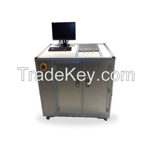
DYALD
FOB Price:
( Negotiable ) Get Latest Price
Place of Origin:
Taiwan
Price for Minimum Order:
-
Minimum Order Quantity:
1 Unit
Packaging Detail:
Wooden Box complies with International shipping standard
Delivery Time:
90 day
Supplying Ability:
3 Unit per Month
Payment Type:
T/T
Product Group :
Contact Person Ms. Teresa
200, Zili 1st St, Taichung, Wuqi District
|
Description
Atomic
Layer Deposition (ALD) is a new process that can be used to replace
chemical vapor deposition (CVD), plasma-assisted chemical vapor
deposition (PECVD), and sputtering technologies. Atomic layer
deposition is also a type of chemical vapor deposition (CVD)
technology. The difference from CVD is that ALD divides the
traditional CVD reaction process into two half-reactions. One is
the Chemisorption saturation process of the precursors, and the
other is the Sequential surface chemical reaction
process.
The
precursor product and the material surface undergo a continuous,
self-limiting (Self-limiting) reaction. The material is slowly
deposited by reacting with different precursor products separately,
and the substance is plated on the surface of the substrate in the
form of a single atomic layer. The deposition of a material
at (1 ~ 2 ), so the growth of ALD material is controlled in
the thickness range of a single atomic layer, forming a step
coverage and large area uniformity.
Atomic
layer deposition has the characteristics of high density, high
thickness uniformity, high step coverage, low temperature process
and atomic-level precise thickness control. In addition to
ultra-thin and high-dielectric material coating, it can also target
tiny circuit structures. Provide hole filling ability, such as the
structure with high aspect ratio and related areas to provide a
uniform thickness coating. Atomic layer deposition is a key
semiconductor device assembly method, and it can also become a
future development area in some nano material synthesis methods,
including semiconductor integrated circuits,
micro-electromechanical, thin-film transistors, OLED displays and
component packaging.
|Specifications
| Model | ALD T*0 | ALD PT*0 | ALD T**0 | ALD T**0 |
| Applicable substrate size | 2 | 2 | 4 | 8 |
| Precursor pipeline | 3 | 3 | 5 | 5 |
| Range of working temperature | RT~**0℃ | |||
| Plasma power | NA | **0 | NA | NA |
| Process materials | Oxide、Sulfide | Oxide、Nitride | Oxide、Sulfide | Oxide、Sulfide |
| Features
| Country: | Taiwan |
| Model No: | DYALD |
| FOB Price: | ( Negotiable ) Get Latest Price |
| Place of Origin: | Taiwan |
| Price for Minimum Order: | - |
| Minimum Order Quantity: | 1 Unit |
| Packaging Detail: | Wooden Box complies with International shipping standard |
| Delivery Time: | 90 day |
| Supplying Ability: | 3 Unit per Month |
| Payment Type: | T/T |
| Product Group : | Functional Coating Equipment |


Coil Coating Machine Production Line(Alubond&Alucobond)")


